- 您现在的位置:买卖IC网 > Sheet目录513 > SI7457DP-T1-GE3 (Vishay Siliconix)MOSFET P-CH D-S 100V PPAK 8SOIC
Si7457DP
Vishay Siliconix
P-Channel 100-V (D-S) MOSFET
PRODUCT SUMMARY
FEATURES
V DS (V)
- 100
R DS(on) ( Ω )
0.042 at V GS = - 10 V
0.045 at V GS = - 6 V
I D (A) a
- 28
- 28
Q g (Typ.)
67 nC
? Halogen-free According to IEC 61249-2-21
Available
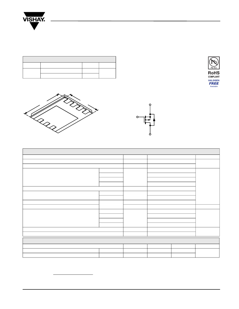
? TrenchFET ? Power MOSFET
PowerPAK SO-8
6.15 mm
1
S
S
5.15 mm
S
2
3
S
G
8
D
7
D
6
D
5
D
4
G
Bottom View
Ordering Information: Si7457DP-T1-E3 (Lead (Pb)-free)
Si7457DP-T1-GE3 (Lead (Pb)-free and Halogen-free)
D
P-Channel MOSFET
ABSOLUTE MAXIMUM RATINGS T A = 25 °C, unless otherwise noted
Parameter
Drain-Source Voltage
Gate-Source Voltage
T C = 25 °C
Symbol
V DS
V GS
Limit
- 100
± 20
- 28
Unit
V
Continuous Drain Current (T J = 150 °C)
T C = 70 °C
T A = 25 °C
I D
- 25.2
- 7.9 b, c
Pulsed Drain Current
Continuous Source-Drain Diode Current
Avalanche Current
Single-Pulse Avalanche Energy
T A = 70 °C
T C = 25 °C
T A = 25 °C
L = 0.1 mH
I DM
I S
I AS
E AS
- 6.3 b, c
- 35
- 28 a
- 4.3 b, c
- 40
80
A
mJ
T C = 25 °C
83
Maximum Power Dissipation
T C = 70 °C
T A = 25 °C
P D
53
5.2 b, c
W
T A = 70 °C
3.3 b, c
Operating Junction and Storage Temperature Range
Soldering Recommendations (Peak Temperature) d, e
T J , T stg
- 55 to 150
260
°C
THERMAL RESISTANCE RATINGS
Parameter
Symbol Typical Maximum Unit
Maximum Junction-to-Ambient b, f t ≤ 10 s
Maximum Junction-to-Case (Drain) Steady State
R thJA
R thJC
19 24
1.2 1.5
°C/W
Notes:
a. Package Limited.
b. Surface Mounted on 1" x 1" FR4 board.
c. t = 10 s.
d. See Solder Profile ( www.vishay.com/ppg?73257 ). The PowerPAK SO-8 is a leadless package. The end of the lead terminal is exposed copper
(not plated) as a result of the singulation process in manufacturing. A solder fillet at the exposed copper tip cannot be guaranteed and is not
required to ensure adequate bottom side solder interconnection.
e. Rework Conditions: manual soldering with a soldering iron is not recommended for leadless components.
f. Maximum under Steady State conditions is 65 °C/W.
Document Number: 73431
S09-0273-Rev. C, 16-Feb-09
www.vishay.com
1
发布紧急采购,3分钟左右您将得到回复。
相关PDF资料
SI7460DP-T1-GE3
MOSFET N-CH 60V 11A PPAK 8SOIC
SI7461DP-T1-GE3
MOSFET P-CH 60V 8.6A PPAK 8SOIC
SI7462DP-T1-GE3
MOSFET N-CH D-S 200V 8-SOIC
SI7465DP-T1-GE3
MOSFET P-CH 60V 3.2A PPAK 8SOIC
SI7530DP-T1-GE3
MOSFET N/P-CH 60V PWRPAK 8-SOIC
SI7620DN-T1-GE3
MOSFET N-CH 150V 13A 1212-8
SI7625DN-T1-GE3
MOSFET P-CH D-S 30V 1212-8 PPAK
SI7629DN-T1-GE3
MOSFET P-CH 20V 1212-8 PPAK
相关代理商/技术参数
SI7458DP
制造商:VISHAY 制造商全称:Vishay Siliconix 功能描述:N-Channel 20-V (D-S) Fast Switching MOSFET
SI7459DP-T1
制造商:Vishay Intertechnologies 功能描述:P-Ch PowerPAK SO-8 30V 6.8mohm@10V
SI7459DPT1E3
制造商:VISHAY 功能描述:Pb Free
SI7459DP-T1-E3
功能描述:MOSFET 30V 22A 5.4W 6.8mohm @ 10V RoHS:否 制造商:STMicroelectronics 晶体管极性:N-Channel 汲极/源极击穿电压:650 V 闸/源击穿电压:25 V 漏极连续电流:130 A 电阻汲极/源极 RDS(导通):0.014 Ohms 配置:Single 最大工作温度: 安装风格:Through Hole 封装 / 箱体:Max247 封装:Tube
SI7459DP-T1-GE3
功能描述:MOSFET 30V 22A 5.4W 6.8mohm @ 10V RoHS:否 制造商:STMicroelectronics 晶体管极性:N-Channel 汲极/源极击穿电压:650 V 闸/源击穿电压:25 V 漏极连续电流:130 A 电阻汲极/源极 RDS(导通):0.014 Ohms 配置:Single 最大工作温度: 安装风格:Through Hole 封装 / 箱体:Max247 封装:Tube
SI7460DP
制造商:VISHAY 制造商全称:Vishay Siliconix 功能描述:N-Channel 60-V (D-S) Fast Switching MOSFET
SI7460DP_09
制造商:VISHAY 制造商全称:Vishay Siliconix 功能描述:N-Channel 60-V (D-S) Fast Switching MOSFET
SI7460DP-T1
制造商:VISHAY 制造商全称:Vishay Siliconix 功能描述:N-Channel 60-V (D-S) Fast Switching MOSFET